FPGA Video card CPU access
In my previous post, I had the VGA output working and was able to display several test patterns. I briefly mentioned that I could read data from the SRAM on the board. From the initial tests of the SRAM, it was displaying a random image as expected with uninitialized RAM but there was a lot of flickering instead of a steady image. This was down to my SRAM controller code taking 3 clock cycles instead of 2. The SRAM controller is currently running at 50Mhz so that means that with 3 cycles on the timing, it puts the time to read the data outside of the VGA timing spec. Fixing the timing for this gave me a nice stable, if random, image. Now that I could display a picture from the RAM the next step is to try to write some data to it.
RAM Access
For accessing data on the VGA card there are two ways that the CPU can control the card. The Register access mode will allow such things as video modes to be set, palettes changes and drawing commands. The Data mode will allow the CPU to have direct access to the Video RAM. I used an extremely basic implementation for the register mode in the last update, where writing the low 2 bits on the data bus was setting the display output mode. This time I want to use the data mode to write a picture to the ram.
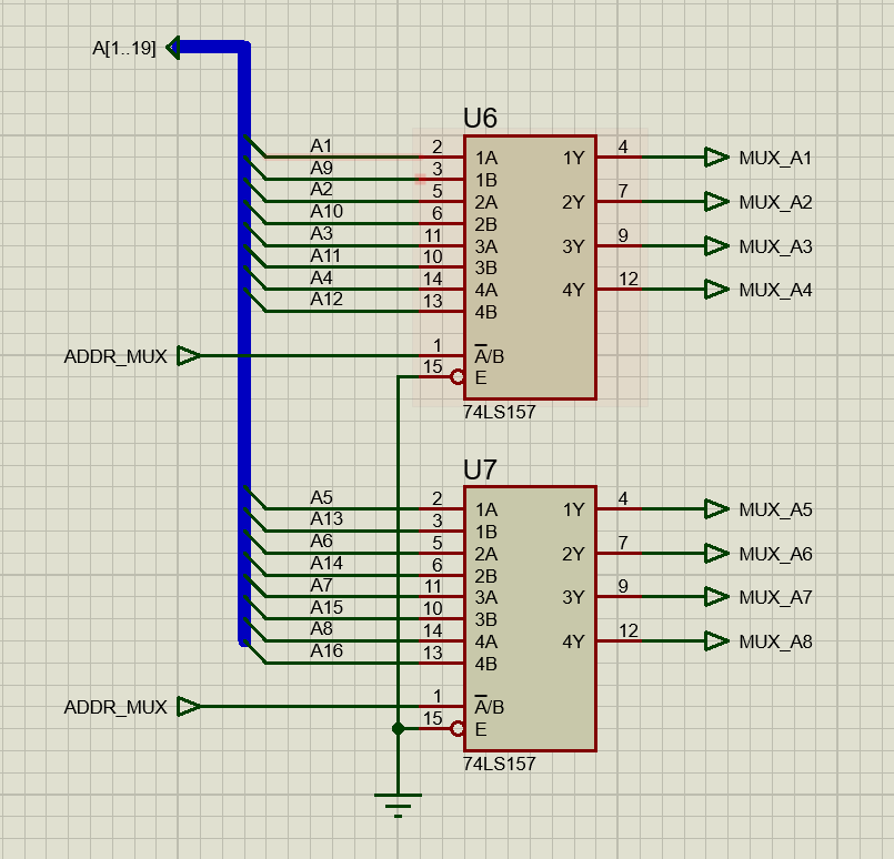
The expansion bus only has address space to allow access to a 1Meg data area on the board. This alone would only allow access to half of the Video RAM but on the actual board this was even further limited by a lack of available pins on the FPGA where only 8 address lines are used. As a workaround for this, a multiplexer on the address bus lines to double the address space. The multiplexer can be used with address lines A1 to A16 are used giving 64K word (128Kb) data access to the device. When used in register mode then the multiplexer is not used so only address lines A1-A8 are active. In that situation A8 is ignored so we have 127 words of data (256B) for the registers.
Although the address multiplexer does allow a bit more of the RAM to be accessed it will still be insufficient to fill the entire picture. Currently the image being display from the SRAM is 640x480x16bit (top 4 bits are not used). To write a full image to the display it would require a 600K of data which is outside the available 128K so a paging scheme will be required for full access. Since the goal of these initial tests is to make sure the hardware is working then just being able to write a small part of the image will prove that.
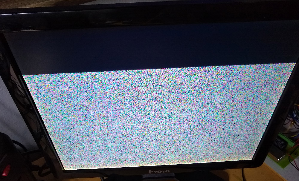
For this test, the FPGA is basically just reading the value from the CPU and passing it straight through to the Video RAM. When the select line is asserted the low half of the address is read and using the 25Mhz clock the upper half of the address bus is read. Once the address is decoded the data is then written to the SRAM. For the first test to keep things simple, the goal is to just write a solid block of colour to the SRAM. Running this test resulted in a nice clear large black bar on the top of the screen.
Displaying Images
With the success of the initial ram access, I thought I would try something a little more ambitious by writing image data to the RAM and get a nice picture displayed. To do this I wrote a small test program to take a 640x480 image and write out the pixel data in a 16-bit raw image format with the 12-bit RGB format. Thinking this was going to be a easy win but running the program displayed the following result.
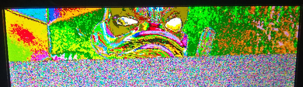
While there is a definite image being displayed, the colours are a very wrong. My initial thought seeing that was my program generating the image data was wrong but after checking the output file it looked correct. I quickly implemented reading of the Video RAM to make sure that the data was being written correctly and the values read back matched the values written so it appeared that it was working as expected.
To track down the problem, I tried a few more images to display and they had the same problem except for a picture with some primary colours in. Those colours seemed to display as expected which was a little confusing. Unfortunately, I didn’t take any photos of some of these tests but another test with a colour gradient for each of the RGB channels did give me an indication of what the problem was. The bit order for each colour should have been in the order of bits 3..0. What was actually being used was in the order 0..3. That explained why the colours were messed up, but primary colours actually displayed correctly. When setting up the pins on the FPGA I had assigned the RGB outputs in the wrong order so after changing that and re-programming the FPGA I tried running my initial image test program again.
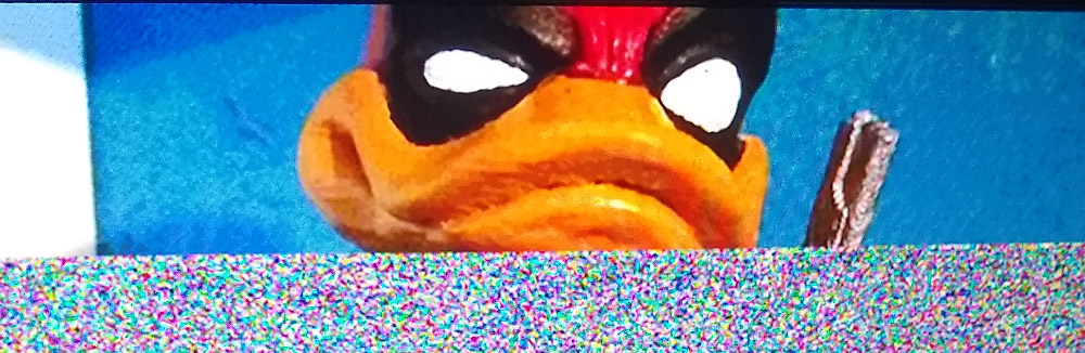
Success!
The picture is now displayed with the correct colours. Now that the colours are fixed the next step is to address the problem that I can only write to a small section of the Video RAM. Writing to the register was currently used to change the video display pattern so it was changed that writing to register 0 still changed the video mode but the next register (address 2) will be used to set the active page in the Video RAM. Setting the page to 0 accesses the 0-128K range of the RAM, settings 1 accesses 128K-256K, etc…
With these changes made, my test program was updated to write the entire picture to the Video RAM, updating the page register every 128K of data. Running this gave me a nice full screen picture.
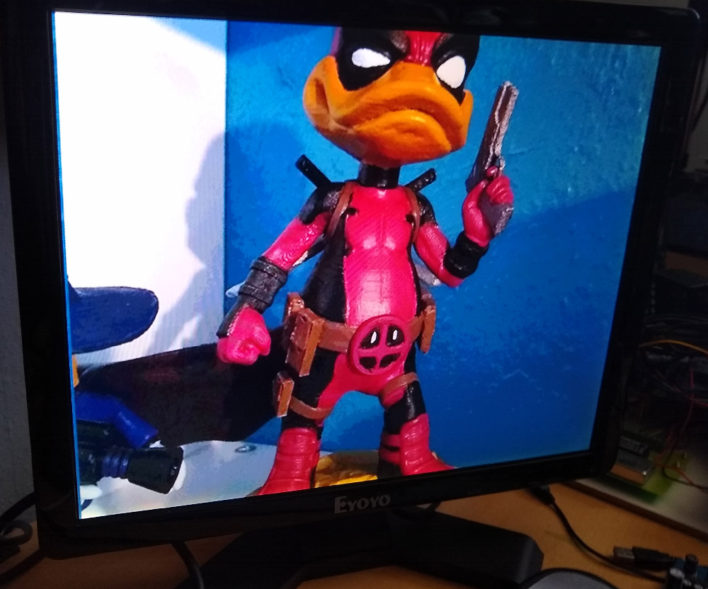
With these tests done it proves that the hardware on the board is fully working. Now that I know that everything is functioning as expected I can start to focus on working on an improved implementation. The FPGA code so far has been focusing on testing the hardware so there are some major issues with it. Writing the full image from a 10Mhz CPU takes approximately 2 seconds so it’s not going to be useable in a functional way currently. The CPU access to Video RAM currently blocks access for the VGA reads so updating the display is causing video artifacts. CPU access is currently taking around 300ns to write to the RAM whereas the VGA controller needs to read it every 40ns. The SRAM controller will need to be able to guarantee access times for the VGA controller without any blocking from CPU or accelerated drawing access.
Before progressing any further I think I will need to develop an initial specification to have some targets to work towards and to get some firm ideas on how I want the video card to operate.