Hardware
Table of Contents
Y Ddraig hardware #
CPU, RAM and ROM #
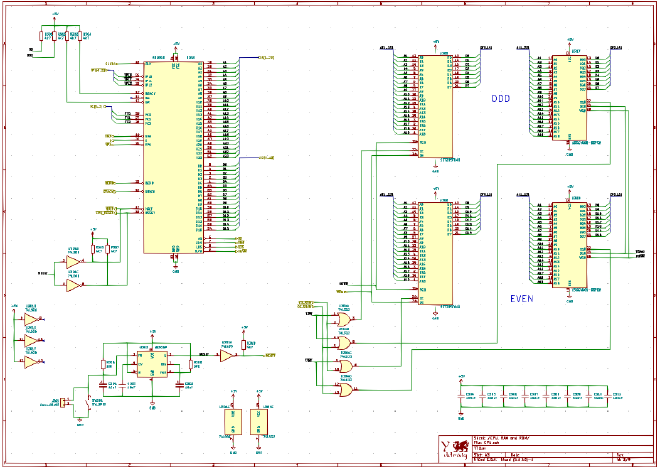
The CPU used by Y Ddraig is the Motorola 68000 running at 10 MHz. The 68000 has a 16-bit data bus and 24-bit address bus internally runs as a full 32-bit machine. The 68000 has 8 general purpose data registers D0-D7 and 8 address registers A0-A7. The address register A7 is also used as a special purpose register holding the stack pointer.
There is 512K of EEPROM available supplied by two 256K x 8-bit SST39SF020 devices for the ODD and EVEN addresses.
RAM is provided by two 512K x 8-bit AS6C4008 Static RAM devices giving a total of 1024K of available memory. There is also the option of adding an additional Dynamic RAM to expand the memory up to a total of 9MB.
Memory Mapping #
As the 68000 is a memory mapped device the address decoding is handled by a Xilinx XC95C108 CPLD. In addition to the address decoding the CPLD is also used as the DRAM controller.
The memory map is as follows:
| Device | Start Address | End Address |
|---|---|---|
| Static Ram | 0x000000 | 0x0FFFFF |
| Dynamic RAM | 0x100000 | 0x900000 |
| Slot1 Data | 0xA00000 | 0xAFFFFF |
| Slot2 Data | 0xB00000 | 0xBFFFFF |
| Slot3 Data | 0xC00000 | 0xCFFFFF |
| Slot4 Data | 0xD00000 | 0xDFFFFF |
| DUART | 0xF7F000 | 0xF7F0FF |
| PIT | 0xF7F100 | 0xF7F1FF |
| KBD | 0xF7F200 | 0xF7F2FF |
| IDE | 0xF7F300 | 0xF7F3FF |
| RTC | 0xF7F400 | 0xF7F4FF |
| Slot1 | 0xF7F500 | 0xF7F5FF |
| Slot2 | 0xF7F600 | 0xF7F6FF |
| Slot3 | 0xF7F700 | 0xF7F7FF |
| Slot4 | 0xF7F800 | 0xF7F8FF |
| ROM | 0xF80000 | 0xFFFFFF |
Dynamic RAM #
Y Ddraig support up to a maximum of 8MB Dynamic RAM via two 4MB 30-Pin SIMMs. Smaller values can be used but both SIMMS must be of the same size.
The XC95108 CPLD handles read and write access to the DRAM and handles the CAS-before-RAS refresh. Any wait states that must be added are done using the DRAM DTACK signal.
Serial port #
A RS-232 serial port is provided using a MC68681 Dual Universal Asynchronous Receiver/Transmitter. Although two channels are available in the DUART only a single channel is being used on this design.
Timer and parallel port #
A MC68230 Parallel Interface/Timer is used to provide a programmable timer and the parallel port interface.
Keyboard and mouse #
The keyboard and mouse are connected via the two PS/2 ports at the rear of the computer and are controlled by a VT82C42 keyboard controller, an 80C42 compatible device.
IDE interface #
The IDE interface provides a 16-bit connection to allow a hard drive or a compact flash card (with suitable adaptor) to be used for mass storage. A jumper link connected to pin 20 allows 5 volts to be supplied if using a CF card which is supported by several CF adaptor interfaces.
Real-time clock #
The Real-time Clock is provided by a 4-bit RTC-72421. A battery backup is provided so that the date and time is not lost when the computer is switched off.
Expansion Slots #
There are 4 expansion slots on the board. The slots are using 64-pin DIN 41612 type C connectors. Each expansion slot is mapped to two memory ranges, a 256-byte address range that can be used to access/control devices connected to the slot. The top word of the address range is reserved as a board ID, so the type of board connected can be identified. The second memory range is a 1 Megabyte range which can be used if a device can’t be mapped to the 256-byte limit or for something that needs direct memory access such as memory expansion.
Expansion slots 1-3 can generate interrupts to the CPU but slot 4 does not support interrupts.
The pinout on the expansion slots are as follows:

Each board has a 8 byte expansion ID. The ID uses the top 4 bits to identify the board type and the lower four bits to identify the board itself.
Currently the boards are mapped to the following IDs
| Type | Identifer | Board |
|---|---|---|
| 1 | 1 | V9958 VDP Video board |
| 1 | 2 | V9990 VDP Video board |
| 1 | 3 | Custom FPGA Video board |
| 1 | 4 | TMS9918 Video board |
| 2 | 1 | YM2151 Audio board |
| 2 | 2 | YM2612 Audio board |
| 3 | 1 | RTL8019AS Ethernet board |
| 4 | 1 | Floppy Drive controller board |
| 4 | 2 | Megadrive Joypad controller board |
Interrupts #
There are three input pins available on the 68000, called IPL0, IPL1, and IPL2. IPL stands for Interrupt Priority Level and each has a priority with 7 being the highest priority. These can be masked by the IPL bits in the status register. The interrupt priority is generated using a 74LS148 8-to-3-line line encoder.
The non-maskable interrupt can be triggered using the J4 header on the PCB.
Interrupt table
| Priority | Interrupt |
|---|---|
| 0 | Non-maskable Interrupt |
| 1 | Expansion slot 1 |
| 2 | IDE interface interrupt |
| 3 | PIT timer interrupt |
| 4 | Serial port interrupt |
| 5 | Keyboard and mouse interrupt |
| 6 | Expansion slot 2 |
| 7 | Expansion slot 3 |
Board information #
Y Ddraig main PCB #
Schematic

Gerbers Latest gerber files available here
BOM Interactive BOM
Expansion board information #
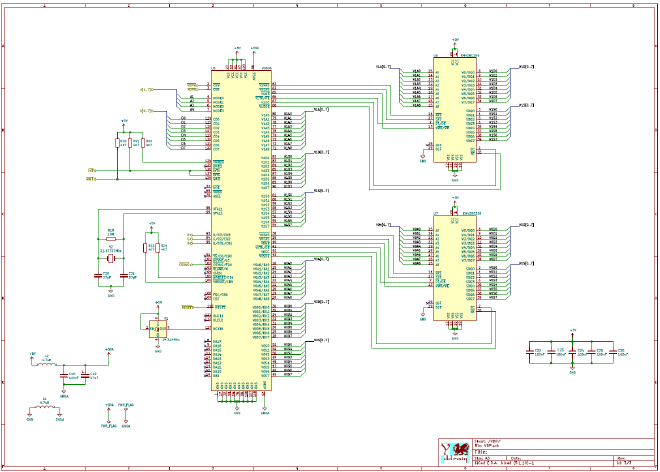
GfxV9990 Video board #
Schematic

Gerbers Latest gerber files available here
BOM Interactive BOM