Problems with the PCBs
Started to assemble the first circuit board and run into some immediate problems. It turns out that there is a short circuit between the 5V and GND planes on the board which is present on the blank PCBs. It’s taken a bit of time to track down where the problem was located but managed to locate the issue at the cost of sacrificing a couple of the circuit boards. Cutting the boards up allowed me to narrow down the location of the fault
The problem was that several vias don’t seem to have any clearance between them and the power planes. Inspecting the files in a gerber viewer doesn’t reveal the issue as it’s showing that the vias have clearance on the two inner planes as expected.
By placing a bright light under the board it’s possible to see where the problem vias are and that there is no clearance with the power planes. The ones highlighted in green are correct and have no issue, the ones in red are the ones directly shorting to the inner two layers. I have confirmed this by drilling out these vias and confirming that the direct short between them has gone.
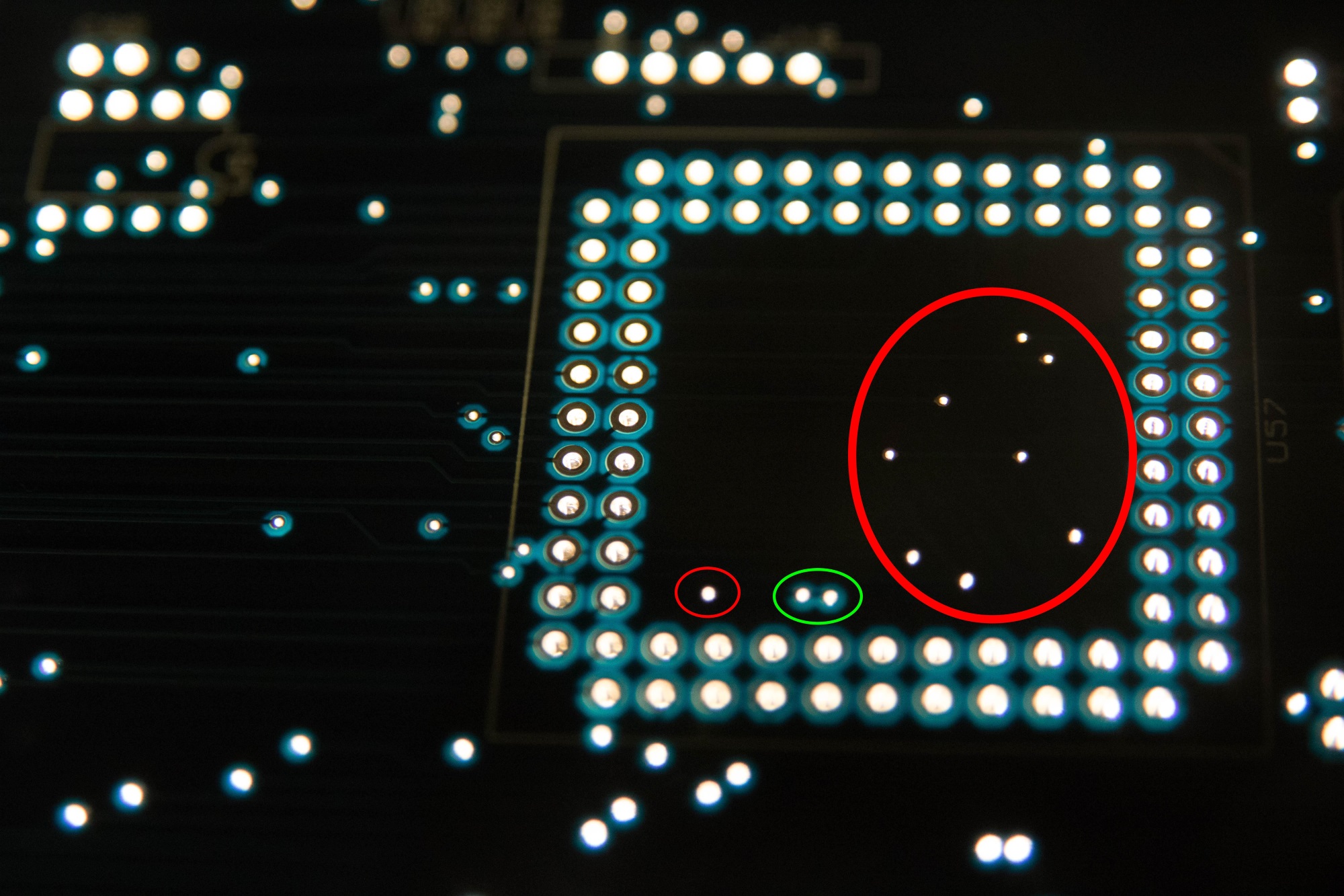
Note: This was tacked down to the software that was used by the manufacturer not loading the gerber files correctly. After we were unable to get a working file they refunded the cost of the boards.